
What is the green mask in PCB?
2024-09-21
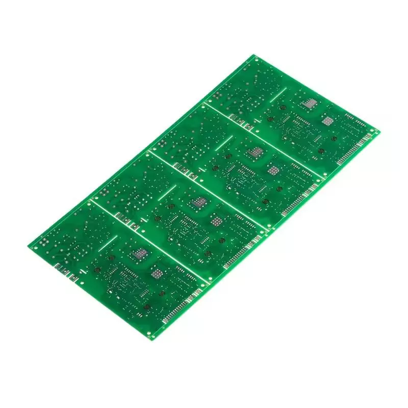
The green mask is applied to the PCB after the solder paste is deposited and reflowed onto the copper contacts. The mask is then exposed to UV light through a photomask, which cures the areas where the traces and pads are desired. The uncured areas are then washed away with a solvent, leaving the green mask as a protective layer. The mask can also be selectively etched away in certain areas to expose the underlying copper for additional processing or testing.
While the green mask is not a new or exotic material, its environmental and technical implications remain important to consider. For example, the pigments used in the mask can contain heavy metals such as lead, cadmium, and chromium, which can pose health risks if not handled properly. Furthermore, the solvents and additives used in the mask can contribute to air pollution and waste generation if not managed effectively. In recent years, there has been a push towards using more eco-friendly and sustainable materials and processes in PCB manufacturing, including alternatives to traditional green masks.